Contents
Overview
The conceptual seeds of the electron microscope were sown in the early 20th century, driven by the fundamental desire to overcome the resolution limits of optical microscopes, which are dictated by the wavelength of visible light. In 1924, French physicist Louis de Broglie theorized that electrons, like light, exhibit wave-like properties, proposing that their wavelength is inversely proportional to their momentum. This groundbreaking idea, later experimentally confirmed by Clinton Davisson and George Paget Thomson in 1927, laid the theoretical foundation. The first practical electron microscope was developed by German physicists Ernst Ruska and Max Knoll in 1931 at the Technical University of Berlin, utilizing electromagnetic lenses to focus electron beams. By 1933, Ruska had built a working prototype that achieved higher resolution than optical microscopes. The first commercial electron microscope, the Siemens Elmiskop I, was introduced in 1939, marking the transition from laboratory curiosity to an indispensable scientific tool, with early applications in understanding materials and biological structures.
⚙️ How It Works
Electron microscopes operate by using a beam of electrons, accelerated to high energies, to interact with a specimen. In a transmission electron microscope (TEM), this electron beam passes through an ultra-thin specimen. The electrons that are transmitted are then focused by a series of electromagnetic lenses onto a fluorescent screen or a digital detector, forming a highly magnified image that reveals the internal structure, morphology, and composition of the sample. For a scanning electron microscope (SEM), the electron beam is scanned across the surface of the specimen. As the electrons interact with the sample, they generate various signals, such as secondary electrons and backscattered electrons, which are detected and used to construct a detailed, three-dimensional-like image of the surface topography. The vacuum environment within the microscope column is crucial to prevent electron scattering by air molecules, ensuring a clear and unimpeded beam path.
📊 Key Facts & Numbers
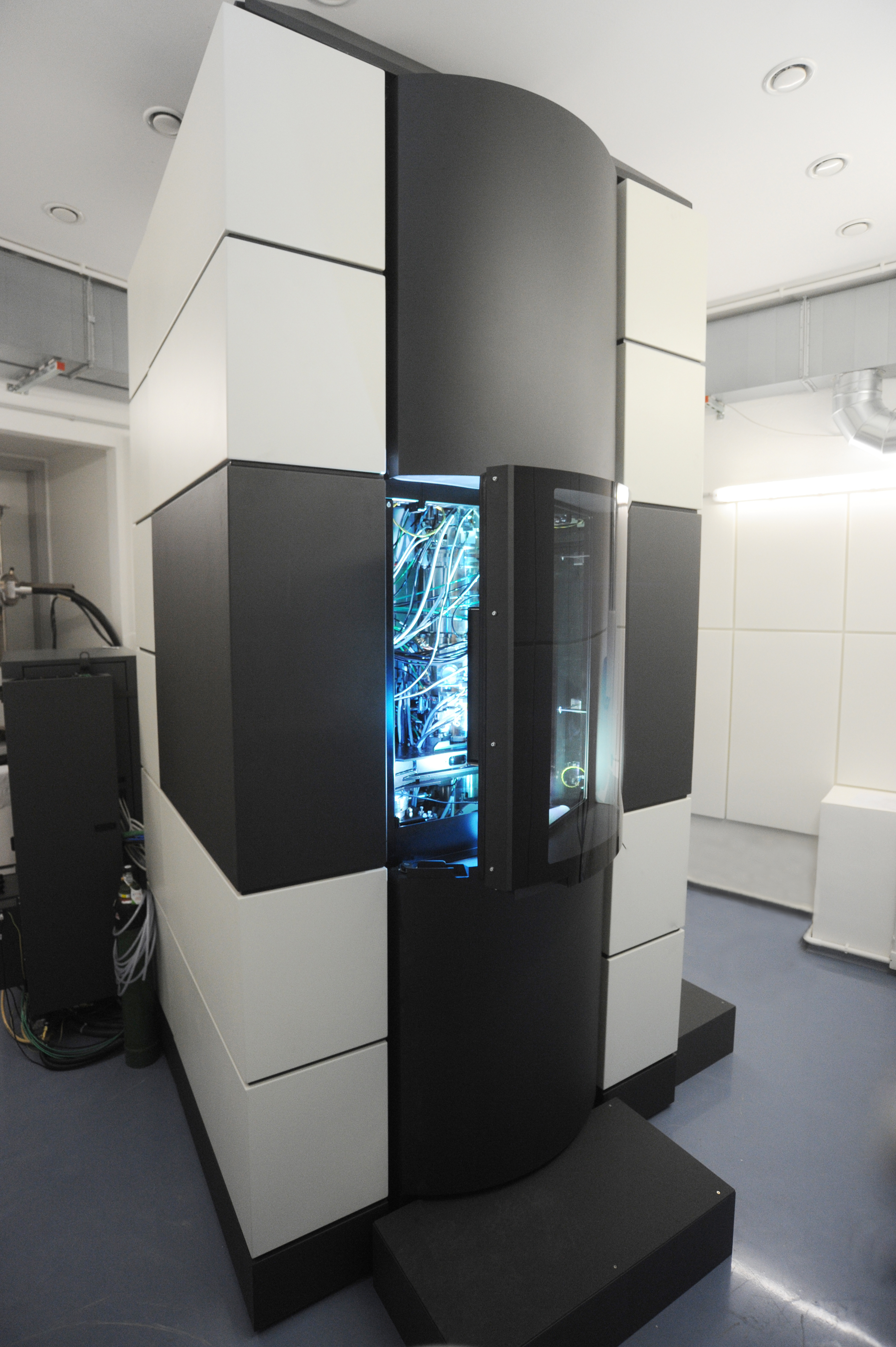
Electron microscopes boast resolutions that are orders of magnitude better than their optical counterparts. Modern TEMs can achieve resolutions of less than 0.1 nanometers (nm), allowing for direct imaging of individual atoms, a feat impossible with light. SEMs typically offer resolutions in the range of 1 to 20 nm, providing exquisite detail of surface features. A single electron microscope can cost anywhere from $50,000 for basic tabletop models to over $1 million for advanced research-grade TEMs. The global market for electron microscopes was valued at approximately $2.5 billion in 2023 and is projected to grow at a compound annual growth rate (CAGR) of around 5% through 2030. These instruments require significant infrastructure, including stable power supplies and vibration isolation, and their operation demands specialized training for at least 100 hours per user.
👥 Key People & Organizations
The development of the electron microscope is inextricably linked to the pioneering work of Ernst Ruska, who, along with Max Knoll, built the first prototype and was awarded the Nobel Prize in Physics in 1986 for his invention. Frits Zernike, though primarily known for the phase-contrast microscope, also contributed to microscopy advancements. Companies like Carl Zeiss AG and Philips (now Hitachi High-Tech) were instrumental in commercializing and refining electron microscope technology, producing iconic models like the Siemens Elmiskop I. In contemporary research, institutions such as Stanford University and the Max Planck Society house state-of-the-art electron microscopy facilities, driving innovation in fields like materials science and cellular biology.
🌍 Cultural Impact & Influence
The impact of electron microscopy on scientific understanding is profound and pervasive. It has enabled breakthroughs in fields as diverse as semiconductor manufacturing, where it's used for quality control and failure analysis, to understanding viral structures like SARS-CoV-2 during pandemics. In biology, TEMs revealed the intricate ultrastructure of cells, leading to a deeper comprehension of organelles like mitochondria and endoplasmic reticulum, and SEMs provided unprecedented views of microorganisms and tissue surfaces. The ability to visualize matter at the nanoscale has been a cornerstone of the nanotechnology revolution, allowing for the design and characterization of novel materials with tailored properties. Its influence extends to art conservation, where it aids in analyzing pigments and degradation processes, and even forensic science, by examining trace evidence with remarkable detail.
⚡ Current State & Latest Developments
Current electron microscopy research is focused on enhancing resolution, speed, and analytical capabilities. Cryo-electron microscopy (Cryo-EM), which allows for the imaging of biological molecules in a near-native frozen state, has seen a dramatic surge in adoption, earning the 2017 Breakthrough Prize in Life Sciences and the 2017 Nobel Prize in Chemistry for its key developers. Developments in aberration correction have pushed TEM resolution to sub-angstrom levels, enabling direct atomic imaging in materials science. Furthermore, correlative light and electron microscopy (CLEM) techniques are becoming increasingly sophisticated, allowing researchers to combine the molecular specificity of fluorescence microscopy with the ultrastructural detail of electron microscopy. The integration of artificial intelligence (AI) and machine learning is also accelerating image processing, analysis, and even automated microscopy operation, with companies like Thermo Fisher Scientific leading these integrations.
🤔 Controversies & Debates
One persistent debate revolves around the interpretation of images, particularly in biological samples where artifacts can arise from sample preparation techniques like fixation and staining. While Cryo-EM has mitigated many of these issues, the inherent complexity of biological systems means that images are not always direct representations of living states. Another area of contention is the accessibility and cost of advanced electron microscopes; while crucial for cutting-edge research, their high price tag and operational demands create a significant barrier for many institutions, leading to a concentration of advanced capabilities in well-funded centers. Furthermore, the ethical implications of high-resolution imaging, particularly in fields like forensics or surveillance, are subjects of ongoing discussion, though less directly tied to the technology's core function.
🔮 Future Outlook & Predictions
The future of electron microscopy points towards even greater resolution, speed, and in-situ observation capabilities. Researchers are developing techniques to image dynamic processes in real-time, such as chemical reactions or the movement of atoms within materials. The push for 'live' electron microscopy, observing samples as they change, is a major frontier. Integration with other advanced analytical techniques, such as spectroscopy, will provide richer, multi-modal data. Furthermore, the development of more compact, user-friendly, and potentially lower-cost electron microscopes could democratize access to nanoscale imaging. The ultimate goal for some is to achieve atomic-resolution imaging of biological molecules in their fully hydrated, functional states, a challenge that continues to drive innovation in sample preparation and imaging techniques.
💡 Practical Applications
Electron microscopes are indispensable tools across a vast spectrum of industries and research areas. In materials science, they are used to characterize the microstructure of alloys, polymers, and ceramics, aiding in the development of stronger, lighter, and more durable materials for aerospace and automotive applications. In the semiconductor industry, SEMs are critical for inspecting integrated circuits for defects, ensuring the reliability of microelectronic
Key Facts
- Category
- technology
- Type
- topic